Imaging the Nanoscale

Presented by

How small can we see?

  • Generally, an unaided human eye cannot see smaller than 40 μm
  • With a good optical microscope, you can clearly see objects of about ½ micron.*
  • With the aid of powerful electronic microscopes, you can basically see/image individual atoms, a fraction of a nanometer.

*The limit is about 200-250 nm, which is 1/2 the wavelength of visible light. However, new optical techniques are pushing the resolution of these microscopes to less than 100nm.

Resolution in microscopy

  • Nanotechnologists have the options to use different types of microscopes, each one with different resolution. 
    • They will choose the appropriate microscope depending on the size of the features they need to clearly image.

Visualization and imaging range: The optical resolution limit of the human eye is about 40 µm. The chart shows the range of electron microscopes, light microscopes, and unaided eye.
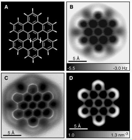
What is possible with modern microscopy?

Imaging molecules -1

Pentacene: C22H14 

Resolution is as low as 5 Å (Ångström = 0.1 nm)!! 

Imaging molecules -2

  • A shows the structure of the molecule.


  • B, C, and D are microscope images (AFM).
    • Notice how you can practically see the C-C and C=C bonds!

Imaging hydrogen bonds

8-hydroxyquinoline (8-hq) molecular assemblies on a Cu substrate.

Imaging chemical reactions

You can take photos of your reagents and reaction products as they form!

Imaging the DNA double helix

Direct Imaging of DNA Fibers: The Visage of Double Helix

Nano Lett., 2012, 12 (12), pp 6453–6458; November 22, 2012

Overview of microscopy

Nanotech All Around Us

Optical microscopes

Biology microscope

Confocal microscope

Probe microscopes

Electron microscopes

Atomic Force Microscope (AMF)

Scanning Tunneling Microscope (STM)

Transmission Electron Microscope (TEM)

Scanning Electron Microscope (SEM)

Comparing optical, electron, and probe microscopes

Resolution Options

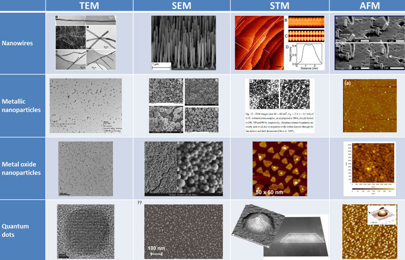
Choose the optimal microscopy technique based on:

  • Size of the sample (what resolution do you need?: Do want an overview image? Or do you want to see a specific detail? 
  • Details you want to learn (surface shape and features, electron density, 2D or 3D image).

Note: Besides resolution, you must consider sample preparation when choosing a microscope technique (Can it be dried? Can it go under vacuum? Can it be sliced? Is it conductive?).


Review of magnification & scale bar

  • Typical images TEM, SEM, STM and AFM images include information about the image, such as scale bar, magnification, and other essential details to better understand the image. Remember the definition of:
    • Magnification, the ratio between size of object on a picture and its real size. 
    • Scale bar,  a bar of known length displayed on a picture as a reference to derive the size of the imaged objects/items. 

Electron microscopy

What is an electron microscope (EM)?

  • An electron microscope (EM) is a type of microscope that uses an electron beam to illuminate a specimen and produce a magnified image. 
  • Only black/white images, but often artificially colored to give a better visual impression.
  • TEM and SEM are two types of electron microscopes


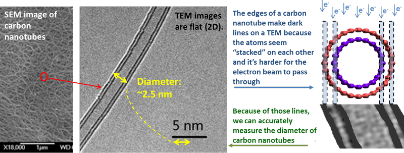
Transmission Electron Microscopy (TEM) 

Probe microscopes

Electron microscopes

Atomic Force Microscope (AMF)

Scanning Tunneling Microscope (STM)

Transmission Electron Microscope (TEM)

Scanning Electron Microscope (SEM)

What is a TEM? 

TEM is a electron microscopy technique where:

  • A beam of high energy electrons is transmitted through the sample. 
  • Transmitted electrons are converted to light to form an image (similar to how an x-ray works).
  • Generate a two dimensional, grayscale image.
  • Needs to operate in vacuum.

More on TEM

  • What is measured?: Direction and energy of the electrons coming out (transmitted) from the sample.
  • Sample:  Must be very thin, 100 nm or less, making sample preparation very tedious.
  • TEM Resolution:  50 pm. Can see individual atoms.
    • High resolution is possible because the wavelength of high energy electrons is just a few picometers (Compare this to optical microscopy!). 
  • Typical information obtained:
    • Internal compositional and crystalline information. 
    • Analyze structure and texture on a molecular level, making it possible to study very fine details.
    • Accurate 2D data regarding diameter of nanotubes, nanowires, and nanoparticles.

TEM Images

  • The lighter areas of the image represent the places where a greater number of electrons were able to pass through the sample. 
  • Darker areas reflect the dense areas of the object. 
  • These differences provide information on the structure, texture, shape, and size of the sample. 

TEM Images

  • Only provide 2D shape information about the sample.
    • Ex: Cannot tell if the item imaged is of something flat, square, tubular, etc. 
    • Does give very accurate 2D measurements.

Example of TEM images -3

It is possible to image biological entities by TEM.
However, these are “dead” or “become inactive” as they are placed under vacuum and illuminated with high energy electrons.

Unless you are told the microscopy technique and what is imaged, it is not easy to say that these are TEM images.

Electron Microscopy

Electron microscopy recently in the news!

  • Scientists were finally able to image a tiny bacteria that was long debated if it even existed. 
  • This bacteria is believed to be the smallest living  thing on earth. 

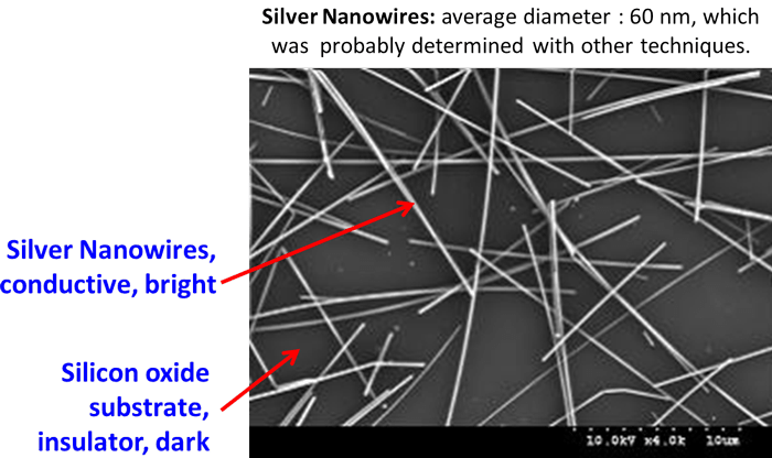
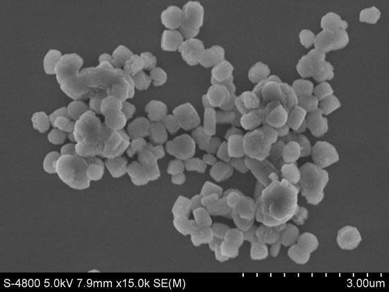
Scanning Electron Microscopy (SEM)

Probe microscopes

Electron microscopes

Atomic Force Microscope (AMF)

Scanning Tunneling Microscope (STM)

Transmission Electron Microscope (TEM)

Scanning Electron Microscope (SEM)

What is an SEM?

SEM is an electron microscopy technique where:

  • A beam of low energy electrons is scanned over a sample. The electrons do not go through the sample but bounce off its surface
  • Scattered electrons are analyzed by a detector to produce a 3D, grayscale image of the surface of the sample.
  • Operates under vacuum.

More on SEM

  • What is measured?: Energy of the scattered electrons bouncing off the surface of the sample.
  • Sample: Does not require much preparation for solid, inorganic samples. Biological samples require a more extensive preparation.
  • SEM resolution: typically ~5-10 nm.
  • Information obtained:  
    • Three-dimensional images give understanding of the shape of the sample.
      • The sample can be rotated around to obtain various views and image from all sides.
    • Details of the surface.
    • Does not provide info on anything below the surface, no info on the internal structure. 
      • Example: from an SEM image, you won’t be able to tell if it’s a rod or pipe (hollow inside).


SEM Images

Bright areas indicate surfaces that reflect electrons very well, typically metallic/conductive surfaces. Dark area mean non-conductive surfaces. 

Example:

  • Metal surfaces appear bright.
  • Ceramics appear darker.


Note: Do not compare the brightness of two items if they are not on the same image!

Examples of SEM Images

  • Note:
    • All these images are 3D and grayscale.
    • The scale bar is in the order of μm, much larger than the bar of TEM images.


Images taken with the sample tilted at an angle

TEM/SEM Differences

  • TEM can give much higher resolution, but images are flat (2D).
  • SEM 3D images provide more information about the shape of features and also about the location of features relative to each other.

SEM

SEM

TEM

TEM

Probe Microscopy

What is a probe microscope (PM)?

  • Scanning probe microscopes (SPM) are a class of microscopes used to study the surface character of materials.
  • They scan the surface the same way you would scan a surface with your finger.  
  • STM and AFM are two types of probe microscopes.

How does probe microscopy work?

Works similarly to a blind person reading the Braille alphabet. A probe tip “reads” the surface by “feeling” it, similarly to a Braille pattern.

  • Every little bump it feels on the surface is translated into images.
  • It’s possible to “feel” individual molecules.
    • STM “feels” an electrical current between the probe and surface.
    • AFM “feels” the force between the probe and surface.

Scanning Tunneling Microscopy (STM)

Probe microscopes

Electron microscopes

Atomic Force Microscope (AMF)

Scanning Tunneling Microscope (STM)

Transmission Electron Microscope (TEM)

Scanning Electron Microscope (SEM)

What is an STM?

  • STM is an probe microscopy techniques where:
    • A small metallic tip/probe “interrogates” the surface of the sample via an electric current. 
    • As the probe moves around the surface, the amount of current measured is proportional to the structure’s height. 
    • A computer generates an image based on the position of the tip and the current generated.
      • Ex: If an atom projects out of the surface, then a higher electrical current will flow through the tip and the computer will convert the increase in current to an increase in height when making the image.
    • It is possible to visualize and move around individual atoms.


More on STM

  • What is measured?: The electrical current  between the surface and the probe, also called the “tunneling current”. 
    • When a conducting tip is brought very near to the sample surface, a voltage difference applied between the two can allow electrons to tunnel through the vacuum between them. 
    • The resulting tunneling current is a function of tip position, applied voltage, and the nature of the atoms/molecules on the surface. 
  • Sample: Since the signal measured is an electric current, samples must be conductive, or coated.
    • Can be done in vacuum, air, or water, and at a wide range of temperatures (0K to 100s+ C).
  • STM resolution: 0.1-0.2 nm, individual atoms are imaged and manipulated. 
    • For an STM, good resolution is considered to be 0.1 nm lateral resolution and 0.01 nm depth resolution.
  • Information obtained:  
    • Three-dimensional images give understanding of the shape of the sample.
    • Details of the surface (roughness, defects, structural info).
    • Does not provide info on anything below the surface, no internal info.
    • Can pick up and arrange atoms or small molecules.


STM Images

  • Images can show detailed atomic structure. 
  • Images are maps of the surface structure.
  • Since tunneling current also depends on electron density of the sample, STM can give electron density information.


STM Images

  • Color is added to visually emphasize important features.
  • With the precise depth resolution and advanced software for processing images, scientists can color images in many different ways.
    • according to height, curvature or other surface properties.


Examples of STM Images

  • Can image biological molecules.
  • Study the order of atoms in a structure.
  • Discover and study variations and defects.

Maneuvering atoms/small molecules  

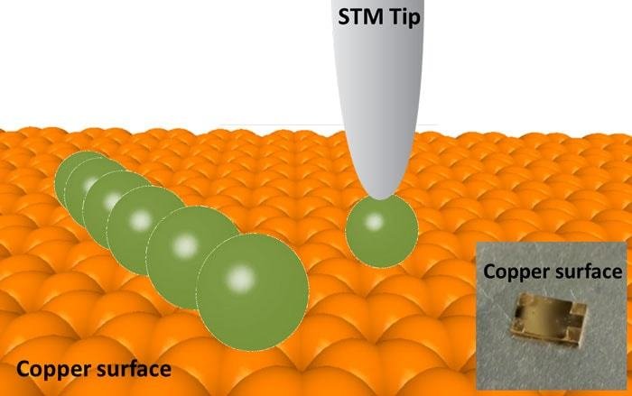
It’s possible to move around atoms and small molecules on a copper surface using an STM.

That’s how this was made…

moving CO molecules around!

Atomic Force Microscopy (AFM)

Probe microscopes

Electron microscopes

Atomic Force Microscope (AMF)

Scanning Tunneling Microscope (STM)

Transmission Electron Microscope (TEM)

Scanning Electron Microscope (SEM)

What is an AFM?

  • AFM is a probe microscopy technique where:
    • A small tip on the end of a cantilever scans, in a grid fashion, across the sample to generate images by “feeling” the surface. 
    • As the tip scans across, the attraction/repulsion force between the atoms on the tip and the atoms on the surface causes the cantilever to bend by minute, but measurable, amounts. 
    • The grid position and amount the cantilever bends is used to generate a 3D image of the surface. 
    • It is possible to visualize and move around individual molecules.

AFM cantilever tip

More on AFM

  • What is measured?: The movement of the cantilever caused by the force between the atoms on the probe tip and the atoms on the sample surface
  • Sample: Anything dry on a surface (no vacuum, no conductivity restriction).
  • AFM resolution: 0.1-0.2 nm, individual molecules.
  • Information obtained:  
    • Three-dimensional images give understanding of
      the shape of the sample.
    • Details of the surface related topography:
      Smoothness, roughness.
    • Very accurate information on the vertical access
      can be obtained and used as dimensional data.
    • Cannot use dimensions on the lateral plane as accurately.
    • Does not provide info on anything below the surface, no internal info.
    • Can pick up and arrange small molecules.
  • The AFM is one of the most important tools for imaging, measuring, and even manipulating nanomaterials. 


Ultra-high resolution probe tips

Nanotechnology made it possible!

Major advancements in microscopy were facilitated by nanotechnology.

  • By using a carbon nanotube, the tip gets so small and sensitive it is now possible to see molecules.


AFM Images

  • Colored lighter or darker based on the distance or force from the surface.
    • Legends help you visualize distance from surface by color. 
  • Other info generated by software such as dimensions, roughness profile etc..
    • Surface morphology: Accurate mapping of the surface roughness.

AFM Images

  • 3D images are generated to give good visuals of surface  roughness using color and mapping.

More on AFM Images

  • Vertical information:  
    • AFMs are very good at providing information regarding the “height” of nanoscale objects present on a surface. 
    • Parameter of nanomaterials, such as the diameter of carbon nanotubes or nanowires, can be determined by observing the nanotube under the AFM. 
    • Curiously, the diameter is determined by looking at the “height” rather than at the “width” of the nanotube.

More on AFM Images

  • AFMs are used in studying thin film roughness.
    • Ex: for use in electronics – like flexible displays.
      • Smoothness/low roughness is an important quality.

More on AFM Images

  • Planar information: AFMs provide information about the atomic look of the sample surface.
    • Surface morphology (roughness) at the atomic level lets us see the shapes of molecules.

Summary of Microscopy

Summary Table

How do nanomaterials look? 

How do nanomaterials look?

This lesson was presented by: 

To learn more about nanotechnology, visit omninano.org

Imaging the Nanoscale

By Omni Nano

Imaging the Nanoscale

Investigating and imaging Nanomaterials

  • 8,692